
GE DS215TCDAG1BZZ01A Digital I/O Board Mark V with Firmware


Introduction:
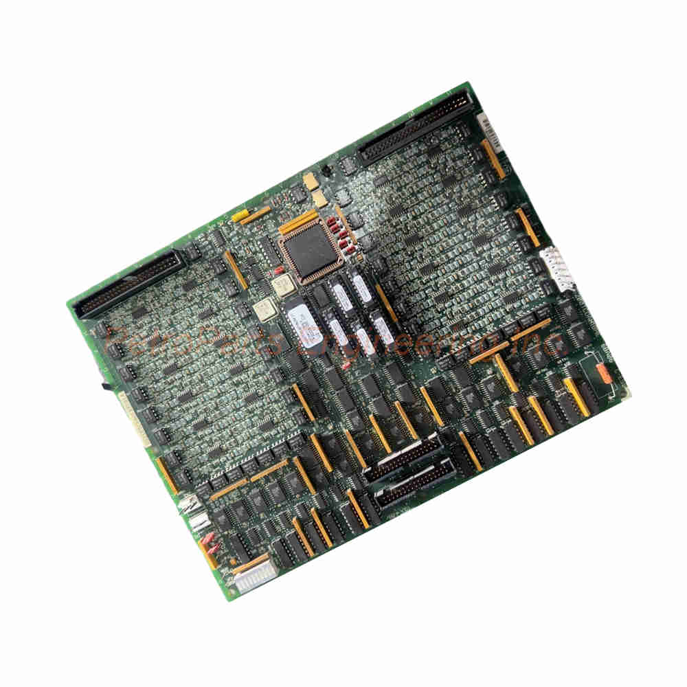
GE DS215TCDAG1BZZ01A digital I/O board with firmware for Mark V. Processes DTBA/DTBB contact inputs and TCRA relay outputs. Features IONET communication.
 Customer Reviews
UBEST Automation – Trusted Global Automation Parts Supplier
We offer a wide range of in-stock industrial automation spare parts. All products come with a 12-month warranty and a 30-day refund for quality issues.
Product Attributes:
Notice: For real-time prices and inventory, please click the button below to contact us.
GE DS215TCDAG1BZZ01A Digital I/O Board with Firmware
The GE DS215TCDAG1BZZ01A is a digital I/O board with firmware from General Electric. This board belongs to the Mark V control system series. The manufacturer designed this board to process digital contact input signals and contact output signals. The United States (USA) manufactures this board. Consequently, it plays a vital role in turbine control applications as part of GE’s Speedtronic Mark V series.
Functional Overview of the DS215TCDAG1BZZ01A
The GE DS215TCDAG1BZZ01A resides in digital I/O cores Q11, Q51, and Q21 when present. The board processes contact input signals from the DTBA and DTBB terminal boards. Additionally, it processes contact output (relay/solenoid) signals from these two boards. The signals then travel through the IONET to the TCQC board in R1 or R2. Furthermore, signals also go to the CTBA terminal board in R5. For this reason, the board serves as a central I/O processor within the Mark V architecture.
The GE DS215TCDAG1BZZ01A is not the original device of its functionality. Instead, it edits the original DS215TCDAG1 parent circuit board. This board adopts a B-rated significant functional product revision. It also includes an optional software package (ZZ01A). Consequently, this board offers enhanced capabilities over the base version.
Technical Specifications of the DS215TCDAG1BZZ01A
General Specifications
The GE DS215TCDAG1BZZ01A is a digital I/O board from the Mark V series. Reference manual GEH-6195 provides documentation for this board. The board includes optional firmware designated ZZ01A. This revision represents one revision level. The functional product abbreviation is TCDA.
Hardware Jumpers Configuration
The GE DS215TCDAG1BZZ01A features eight hardware jumpers for configuration. J1 and J8 serve factory testing purposes only. J2 and J3 connect IONET termination resistors. J4, J5, and J6 configure the board’s IONET ID. J7 controls the stall timer function. Therefore, proper jumper configuration is essential for correct board operation.
Software Configuration
SDCC contains the primary control circuits and software for the drive. The GE DS215TCDAG1BZZ01A also includes general-purpose interface circuits. These circuits connect to other boards to form different types of AC and DC motor drives. The interface circuits control and process drive signals, motor signals, and customer I/O. Additionally, I/O configuration constants for contact input inversions are entered in the HMI’s I/O Configuration Editor.
Contact Input Circuits
Contact inputs from the DTBA and DTBB terminal boards route to the GE DS215TCDAG1BZZ01A via the JR and JQ connectors. The board’s circuitry conditions these incoming signals. It then timestamps any changes in state. Finally, it sends the conditioned signals to the IONET via the JX1 (or JX2) connector. The board performs contact signal inversions using software and I/O configuration constants.
Connector Descriptions
JP Connector (Power Distribution)
The JP connector serves as a power distribution channel within the system. Power originates from the TCPS board. The GE DS215TCDAG1BZZ01A routes this power via the R1, R2, and R5 cores to reach Q11, Q21, and Q51 cores. Consequently, the JP connector ensures that designated cores receive the necessary electrical supply to function optimally.
JQ Connector (DTBA Inputs)
The JQ connector establishes a link between the DTBA board’s JQR socket and the I/O boards. It transports contact input signals from the DTBA to the GE DS215TCDAG1BZZ01A. This communication pathway enables the TCDA board to receive and process input signals generated by the DTBA.
JR Connector (DTBB Inputs)
Similar to the JQ connector, the JR connector links the DTBB board’s JRR socket to the I/O boards. It transmits contact input signals from the DTBB to the GE DS215TCDAG1BZZ01A. By establishing this connection, the system enables seamless data transfer between the DTBB and the I/O board.
JO1 and JO2 Connectors (Output Signals)
JO1 and JO2 connectors send contact output signals to the TCRA board. These signals often relate to relays or solenoids. JO1 transmits signals to the TCRA board in position four. JO2 transmits signals to the TCRA board in location five. Notably, relays in position four are controlled directly by TCQE in R1 and are not utilized in Q11. For this reason, JO1 typically sees no use in Q11 cores.
JX1 and JX2 Connectors (IONET Signals)
JX1 and JX2 connectors are part of a shielded twisted pair for IONET signals. These connectors play a key role in data transmission between different components. Specifically, the module in the Q11 core writes signals to the JX2 connection on the TCEA board in position five of the P1 core. Similarly, the board in the Q51 core writes signals to the JX connection on the CTBA in the R5 core. Consequently, this communication mechanism enables the exchange of critical signals throughout the system.
Physical Location and Cores
The GE DS215TCDAG1BZZ01A can be found within digital I/O cores Q11 and Q51. When present, Q21 also hosts this board. The board processes output signals coming from the two TCRA boards. It also processes input signals coming from the DTBB and DTBA boards. After processing, these signals normally travel across the IONET to the CTBA terminal board and the TCQC board.
Installation Guidelines for the DS215TCDAG1BZZ01A
First, de-energize the control system completely and follow all lockout/tagout procedures. Then, locate the correct digital I/O core (Q11, Q21, or Q51) for the GE DS215TCDAG1BZZ01A. Before insertion, configure the eight hardware jumpers (J1 through J8) according to your application requirements. Next, align the board with the card guides in the rack. Press firmly but evenly to seat the board fully. After that, connect all required cables to their respective connectors (JP, JQ, JR, JO1, JO2, JX1, JX2). Finally, restore power and verify proper board operation using the HMI.
Package Contents
-
One (1) GE DS215TCDAG1BZZ01A digital I/O board with firmware
-
ZZ01A optional firmware (included)
Common FAQs for the DS215TCDAG1BZZ01A
1. Where does the DS215TCDAG1BZZ01A reside in the Mark V system?
The GE DS215TCDAG1BZZ01A resides in digital I/O cores Q11 and Q51. It may also reside in Q21 when present.
2. What signals does this board process?
The GE DS215TCDAG1BZZ01A processes contact input signals from DTBA and DTBB boards. It also processes contact output signals (relay/solenoid) to TCRA boards.
3. How many hardware jumpers does this board have?
The GE DS215TCDAG1BZZ01A features eight hardware jumpers. J2, J3, J4, J5, J6, and J7 are user-configurable, while J1 and J8 serve factory testing only.
4. What is the purpose of the JX1 and JX2 connectors?
JX1 and JX2 connectors on the GE DS215TCDAG1BZZ01A comprise a shielded twisted pair for IONET signals. They enable critical data transmission between different system components.
5. What documentation covers this board?
Reference manual GEH-6195 provides documentation for the GE DS215TCDAG1BZZ01A. Additionally, Appendix A contains hardware jumper settings information.
Why Choose the GE DS215TCDAG1BZZ01A?
In summary, this digital I/O board delivers comprehensive contact processing capabilities for Mark V turbine control systems. First, the eight configurable hardware jumpers provide application-specific flexibility for termination resistors, IONET ID, and stall timer settings. Second, the multiple connector types (JP, JQ, JR, JO1, JO2, JX1, JX2) support all necessary power, input, output, and IONET communication functions. Third, the board’s presence in Q11, Q21, and Q51 cores allows flexible system architecture. Fourth, the included ZZ01A firmware and B-rated revision offer enhanced functionality over the parent TCDAG1 board. Fifth, the IONET communication pathway ensures reliable data exchange with TCQC and CTBA boards. For these reasons, order the GE DS215TCDAG1BZZ01A today for your Mark V digital I/O requirements.